
- Catalogs
- Bruker Nano Surfaces
- Dektak XTL Stylus Profiler System

- Products
- Catalogs
- News & Trends
- Exhibitions
Dektak XTL Stylus Profiler System

Dektak XTL Stylus Profiler System
- Dual Camera Control: Enhances spatial awareness and simplifies navigation and measurement setup through live video interaction.
- Automation and Operation: Features a 300mm automated encoded XY stage and 360-degree theta for accurate programming and minimized errors using Vision64 Production Interface.
- Data Analysis: Vision64 software supports unlimited measurement sites, 3D mapping, and customized characterization with built-in analysis tools.
- Measurement Technique: Stylus profilometry for 2D and 3D measurements.
- Stylus Sensor: Low Inertia Sensor with N-Lite+ low force technology.
- Sample Handling: Motorized, high-accuracy encoded 300mm XY stage and continuous 360° R-Theta stage.
- Software: Includes Vision64 operation and analysis software with options for automated pattern recognition.
- Environmental Requirements: Operates within 20° to 25°C and ≤80% non-condensing humidity.
- Wafer Applications: Suitable for step height measurements, etching rate determinations, and chemical mechanical polishing.
- Large Substrate Applications: Used for printed circuit boards, window coatings, and wafer masks.
- Glass Substrate and Display Applications: Applicable for AMOLEDs, LCD R&D, and solar coatings.
- Flexible Electronic Films: Measures organic photodetectors and copper traces for touch screens.
Catalog excerpts

L>O Dektak XTL Stylus Profiler System • Gage-Capable QA/QC Profiling for Optimal 300mm Performance Stylus Microscopy Innovation with Integrity
Open the catalog to page 1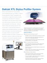
Dektak XTL Stylus Profiler System Bruker’s new Dektak XTL™ stylus profiler accommodates samples up to 350mm x 350mm, bringing legendary Dektak® repeatability and reproducibility to large-format wafer and panel manufacturing. The Dektak XTL features a small footprint with pneumatic passive isolation and a fully enclosed workstation with a wide, easily accessible interlocking door, making it ideal for today’s demanding production floor environments. Its dual-camera architecture enables enhanced spatial awareness, and its high level of automation maximizes manufacturing Though fully optimized for...
Open the catalog to page 2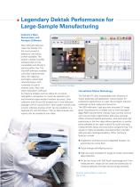
Industry's Best Automation and Analysis Software New software features make the Dektak XTL the most powerful, easiest to use stylus profiler available. The system utilizes Vision64 software that is fully compatible with Bruker's optical profiler line. The Vision64 software enables unlimited measurement sites, 3D mapping, and highly customized characterization with hundreds of built-in analysis tools. Also use Vision Microform software to measure shapes such as radius of curvature. Use pattern recognition to minimize operator error and enhance measurement location accuracy. Data collection and...
Open the catalog to page 3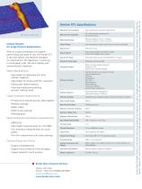
Critical Results for Large-Format Applications With its unique combination of superior performance and ease of use, the Dektak XTL is the new QA/QC and research standard for industrial thin film deposition monitoring in touch-panel, solar, flat panel display, and semiconductor industries. Wafer Applications: - Step height for deposited thin films (metals, organics) - Step height for resists (soft film materials) - Etching rate determinations - Chemical mechanical polishing (erosion, dishing, bow) Large Substrate Applications: - Printed circuit boards (bumps, step heights) - Window coatings -...
Open the catalog to page 4Archived catalogs
 Innova
8 Pages
 Dimension FastScan
8 Pages
 MultiMode 8 Brochure
8 Pages
 Dimension Icon
6 Pages
 Dimension FastScan Bio
4 Pages
 AFM Dimension Edge
8 Pages
 BioScope Resolve
8 Pages
 microflex
6 Pages
 MALDI PharmaPulse HTS
4 Pages
 rapifleX MALDI Tissuetyper
8 Pages
 The new autoflex speed
10 Pages
 PRIME
PRIME12 Pages
 MALDI Biotyper CA System
8 Pages
 MBT STAR-BL Software
4 Pages
 AutoMet AFM Software
2 Pages
 Dimension Icon SSRM
2 Pages
 MultiMode 8-HR
8 Pages


- BRUKER microscope
- BRUKER optical microscope
- BRUKER laboratory microscope
- BRUKER benchtop microscope
- Spectroscope
- BRUKER biology microscope
- Benchtop spectrometer
- BRUKER research microscope
- Fluorescence microscope
- Digital microscope
- BRUKER high-resolution microscope
- Medical microscope
- Inverted microscope
- Compact microscope
- Zoom microscope
- Research spectrometer
- Optical spectrometer
- 3D microscope
- High-resolution spectrometer
- Environmental analysis spectrometer