- Products
- Catalogs
- News & Trends
- Exhibitions
Product Information µCP3.0
1 /4Pages

Product Information µCP3.0
1 /4Pages
Catalog excerpts

μContactPrinter Systems for Microcontact Printing and NIL
Open the catalog to page 1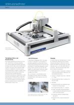
GESIM μContactPrinter Basics Fully automatic GESIM μContactPrinter 4.1 The Making of Micro- and Nanostructures… Few simple methods exist to print tiny structures. One of them, microarray spotting (e. g. with the GESIM Nano-Plotter) generates structures around 100 μm. Microcontact printing (μCP) can work on the nanoscale: PDMS (silicone) is molded on a structured master; the resulting stamp is soaked in sample, dried, and pressed onto the surface, transferring molecules from the protruding areas. Chemicals, biomolecules, nanoparticles, beads, and cells can be printed, which is why μCP is getting...
Open the catalog to page 2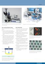
Stamp holder Ink-dry station Print head Substrate holder PVM-A on an inverted microscope, with external UV lamp and electronic/pneumatic Workstations in the semi-automatic μContactPrinter 3.0 control module (right) Semi- and Fully Automatic Systems Some Technical Data GESIM microcontact printers come in different flavours: ■ Stamps, round: 10 mm x 10 mm (Si master chip: 15 mm x 15 mm), 20 mm x 20 mm and for 24-well and 96-well microtiter plates, or customized ■ The process validation module (PVM-A) consists of Z-drive and table (adjustable on an air cushion), for method optimization and other...
Open the catalog to page 3
© M+K Werbeagentur GmbH | www.mkwa.de GESIM μContactPrinter Gesellschaft für Silizium-Mikrosysteme mbH Bautzner Landstraße 45 01454 Großerkmannsdorf, Germany Tel. +49 (0)351 - 2695 322 Fax +49 (0)351 - 2695 320 [email protected]
Open the catalog to page 4All GeSiM catalogs and technical brochures
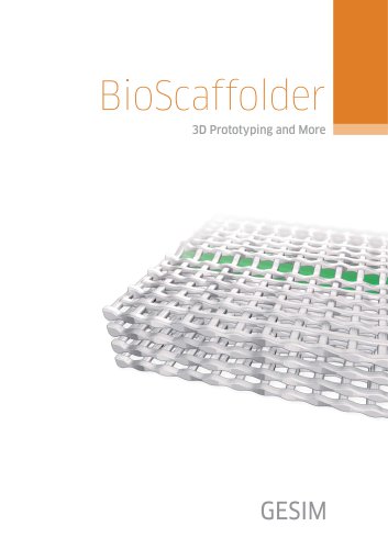 Bioscaffold Printers
4 Pages
 Nano-Plotter catalogue
13 Pages