- Catalogs
- Hamamatsu Photonics France
- ORCA-Fusion
ORCA-Fusion
1 /28Pages

ORCA-Fusion
1 /28Pages
Catalog excerpts

ORCA-Fusion Gen III Scientific CMOS Camera TECHNICAL NOTE Version 1.2 / December 2018 HAMAMATSU
Open the catalog to page 1
TECHNICAL NOTE Table of Contents Table of Contents . . . . . . . . . . . . . . . . . . . . 2 The First Gen III Scientific CMOS Sensor . . . . . . . . . . . . 3 Read Noise and Read Noise Uniformity . . . . . . . . . . . . . 3 CCD and CMOS sensor structure . Read noise and read noise uniformity . What does read noise non-uniformity look like in an image? . Implications of Read Noise and Read Noise Uniformity . . . . . . . 8 Read noise and signal to noise ratio . Low camera read noise improves low-light image quality . Binning and other practical advantages of low read noise . Comparing EM-CCDs...
Open the catalog to page 2
TECHNICAL NOTE The First Gen III Scientific CMOS Sensor The ORCA-Fusion, Hamamatsu’s newest member of the ORCA Family of scientific cameras, utilizes a custom scientific CMOS (sCMOS) sensor designed from the ground up for low-light quantitative imaging. By implementing a custom pixel design in this sensor and by using state-of-the-art semiconductor processes we’ve greatly improved pixel read noise, read noise uniformity and linearity. With these improvements we’ve achieved our goal of creating a camera that outputs beautiful images and quantitative data directly from the camera, especially in...
Open the catalog to page 3
Data output PD: Photo Diode HT: Horizontal Transfer CCD VT : Vertical Transfer CCD FDA : Floating Diffusion Amplifier CDS : Correlated Double Sampling AMP: Amplifier AD : Analog to Digital converter Figure 1. Pixel structure and read out pathway in (A) CCD and (B) CMOS. CCDs and CMOS are both arrays of photodiodes that are able to detect light by converting photons into electrons. The difference in structure between these two technologies leads to important differences in performance and features. In a CCD, the pixel structure is designed to manage the signal in the charge domain. So all the...
Open the catalog to page 4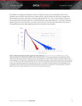
TECHNICAL NOTE An example of a read noise histogram is shown in Figure 2. As you can see, histograms tell a more complete story of CMOS read noise than a single number. Figure 2 shows the read noise histogram for two theoretical cameras, each with a read noise specification of 1.4 e- rms. In this example, Camera A has no pixels with read noise above 8 e- and Camera B has many pixels above 8 e-. If you were choosing between these two cameras there is no way to know from the rms read noise specification that there is this big difference unless data regarding read noise distribution was provided....
Open the catalog to page 5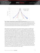
TECHNICAL NOTE Figure 3. Histogram of the pixel output from a single dark image for three simulated cameras. The distribution in the camera output in each pixel in a single dark frame provides a quick glimpse at the extent of read noise heterogeneity. On the x-axis, dark output shows the fluctuation in signal above and below the camera’s offset. The y-axis shows the number of pixels with this value. In this figure, all simulated cameras have a read noise spec of 1.4 e- rms, but Camera B (blue), has large distribution similar to Gen II sensors, both front and back illuminated, Camera A (red) has...
Open the catalog to page 6
orca-Fusion Camera Table 1. Measured distributions of absolute dark output after pixel offset subtraction from a single frame in Gen II, Gen II with correction and Gen III ORCA-Fusion camera. This table addresses the question of pixel read noise uniformity in single frame with measured data. The dark offset of a camera is a known and set value. In a dark image, measuring pixels with values both above and below the offset is a way to examine read noise uniformity. For each camera and mode, we display the number of pixels with an absolute value of the difference between the dark reading and the...
Open the catalog to page 7
TECHNICAL NOTE Implications of Read Noise and Read Noise Uniformity Read noise and signal to noise ratio Pixel signal to noise ratio (SNR) is a standard metric used to express camera sensitivity. For CCDs and sCMOS, pixel SNR is calculated as Equation (1). Note that this equation assumes the exposure time is short, so the dark noise becomes small and negligible, and does not need to be included in the equation. Equation 1. SNR equation for CCD and CMOS. QE is quantum efficiency (%/100), S is input photon number (photons / pixel / s), Ib is background, Nr is read noise (e- rms). This equation...
Open the catalog to page 8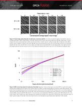
orca-Fusion Read noise (e- rms) C D Figure 5. Visual image quality depends on light levels, read noise and QE. From these simulated images it's possible to see how multiple parameters affect image quality in low light. Panels A and F have 0 read noise at 80% and 100% QE respectively. In these images, the noise is exclusively due to shot noise. So even with a "perfect camera," without enough light, images are noisy. When camera noise is added to a system, even with 100% QE, visual contrast becomes worse. Of course the best scenario is to have both high QE and low noise, but when this is not an...
Open the catalog to page 9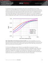
TECHNICAL NOTE To complement Figure 5 images with quantitative data, Figure 6 shows SNR plots for 5 simulated cameras. Such simulated SNR plots are commonly used to show the light intensity where a camera with certain spec is either read noise limited or shot (signal) noise limited. To be shot noise limited means that the noise resulting from the signal is greater than the noise from the camera. In an SNR plot, the shot noise limited regime begins at the light level where the plot trasitions from a curved to a straight line. Figure 6 shows that at low light, a camera with 80 % QE, can outperform...
Open the catalog to page 10
TECHNICAL NOTE Binning and other practical advantages of low read noise Switching from CCDs to CMOS for scientific imaging has many advantages. Lower read noise, larger field of view and faster frame rates are key to sCMOS adoption. But binning is one feature of imaging that is fundamentally altered by the structure of CMOS sensors. In CCDs, charge from the binned pixels is combined before readout and is therefore noiseless. Binning n pixels results in n times the signal with the same read out noise. Thus, at low light, a binned CCD pixel has n times the SNR of the unbinned pixels. For example,...
Open the catalog to page 11All Hamamatsu Photonics France catalogs and technical brochures
 NZConnectMD Scan
3 Pages
 Mini-spectrometer
7 Pages
 ORCA-HALO
3 Pages
 ORCA-QuestlQ
4 Pages
 TDI camera C10000-801
2 Pages
Archived catalogs
 X-ray TDI camera C12300-321
4 Pages
 ORCA-spark
2 Pages
 BT-CCD camera C8000-30
2 Pages
 ORCA Lightning
8 Pages
 digital CMOS camera C14130-20P
12 Pages

- Analysis software
- Visualization software
- Radiology software
- Control software
- Laboratory software
- Windows software
- Camera with USB port
- Spectroscope
- Diagnostic software
- Cloud-based software
- Design software
- Acquisition software
- Capture software
- Traceability software
- Medical camera
- Microscope camera
- Web-based software
- Sharing software
- Server software