- Catalogs
- Hitachi High-Tech Europe GmbH
- Product Catalogue: SEM, FIB, BIB, TEM
- Company
- Products
- Catalogs
- News & Trends
- Exhibitions
Product Catalogue: SEM, FIB, BIB, TEM
1 /31Pages

Product Catalogue: SEM, FIB, BIB, TEM
1 /31Pages
Catalog excerpts

Hitachi’s world of electron microscopy In this overview brochure, we present a wide range of electron and ion beam systems from Hitachi, organised by product class. Each tool is designed to reliably meet your application needs. In 1969, Hitachi began developing field emission (FE) electron beam source technology. In just three years, Hitachi successfully developed an FE-SEM by creating a practical FE technology. Since then, Hitachi’s FE technology has been used for more than 40 years in high-resolution SEMs and TEMs in a variety of fields such as biology, materials science and semiconductor engineering....
Open the catalog to page 2
Electron Sources in the Hitachi SEM families Thermal Tungsten Emitters Lens Types in the Hitachi SEM families Electron Beam Magnetic Lens The preferred choice for general applications from imaging to analysing. Material Tungsten wire with a sharp bend for moulding a tip Operating temperature Virtual source diameter Energy distribution of the electrons ~ 2–3 eV Sample streams Operating hours routine industrial environments where structures down to sub-100 nm are analysed. These emitters backscattered electrons into the lens aperture towards the in-lens detector. Virtual Lens Inlens Detector Electrostatic...
Open the catalog to page 3
Sample handling under inert gas conditions Samples that oxidise or absorb moisture easily should avoid contact with the atmosphere. Otherwise their properties will change. They need strict handling in an inert gas environment before and after preparation. Each tool listed above can be equipped so that complete handling in an inert gas atmosphere is ensured at all times. This is guaranteed by Hitachi’s “air protection” framework. As part of Hitachi’s “air protection” concept, both the IM series and Hitachi SEM can be equipped to ensure complete handling in an inert gas atmosphere at all times....
Open the catalog to page 4
The Optimum Electron Optics Configure 20 your ideal SEM High-Resolution Field Emission SEM Software Extensions Focused Ion Beam Systems Transmission Electron Microscopes Sample Preparation and Cross-Section Preparation
Open the catalog to page 5
1 Thermal Tungsten Emitters VP-SEMs with Thermal Electron Source 2 SU3800 / SU3900 VP-SEM Product Family SEM imaging and elemental analysis in minutes Copper sulphide crystals. 5kV, SE signal 3 High-Resolution Field Emission SEM Corroded copper wire. 10kV, SE signal Al Cosmetic powder, EDX analysis. 15kV Optional Accessories EDX with sensor sizes up to 65mm2 Automatic multi-range image capture (“Multi-zigzag”) Automation via Python scripting or EM Flow Creator Hitachi Map 3D packages for additional functions such as 3D reconstruction, roughness measurement, particle and pore analysis, image processing,...
Open the catalog to page 7
1 Thermal Tungsten Emitters VP-SEMs with Thermal Electron Source SU3800 / SU3900 VP-SEM Product Family Full SEM functionality in a compact, intuitive design 3 High-Resolution Field Emission SEM 4 Focused Ion Beam Systems Optional Accessories Hitachi Map 3D packages for additional functions such as 3D reconstruction, roughness measurement, particle analysis, image processing, and colour segmentation. Product Features 4nm @ 20kV High-resolution electron optics with beam energies between 300eV and 20keV High and adjustable low vacuum up to 100Pa SE and 4+1 segment backscatter detector standard,...
Open the catalog to page 8
SU3800 / SU3800SE SU3900 / SU3900SE Configure your ideal SEM
Open the catalog to page 9
Thermal Tungsten Emitters SU3800 / SU3900 VP-SEM Product Family 2 SU3800 / SU3900 VP-SEM Product Family Modular VP-SEM platform | 2 sample chambers | 2 types of electron optics SU3800 Samples up to 229mm diameter can be fully inspected (SU3900) 3 High-Resolution Field Emission SEM Multiple sample holder for 33 x 15mm Ø stubs Focused Ion Beam Systems GUI with integrated EDX operation Product Features Analysis accessories (EDX, EBSD, µ-XRF, CL, ...) Specialised multiple sample and filter holders Flexible and effective automation of routine tasks via EM Flow Creator Sample airlocks, also for inert...
Open the catalog to page 10
SU3800 / SU3900 VP-SEM Product Family 2 Thermal Tungsten Emitters Two Specimen Chambers / Eucentric Stages: Up to 200mm Ø, 80mm (H), 2kg sample weight on 5 axes Tungsten Hairpin Cathode Up to 300mm Ø, 130mm (H), 5kg sample weight on 5 axes SU3800 / SU3900 VP-SEM Product Family Configure your ideal SEM Schottky Emitter Schottky Field Emitter 3 High-Resolution Field Emission SEM The SU3800/SU3800SE is the versatile, standard version of the product family. It features a large analytical sample chamber with a eucentric sample stage, which can be fully pulled out for quick sample changes. The chamber...
Open the catalog to page 11
SU9000 II 34 MirrorCLEM Software Extensions
Open the catalog to page 12
High-Resolution Field Emission SEM Schottky Emitter Cold Field Emitter High and Ultra-High Resolution Field Emission SEM 2 SU3800 / SU3900 VP-SEM Product Family ...with Schottky Field Emitter ...with Cold Field Emitter Hitachi’s high-resolution Schottky VP FE-SEMs are available in two versions. These differ in terms of the sample chamber and sample stage. Hitachi’s proven cold field emitter with its sharp tip, narrow band emission and long lifetime drives two SEMs optimised for maximum resolution and special analytics: 3 High-Resolution Field Emission SEM Both UHR SEMs use a Schottky emitter...
Open the catalog to page 13
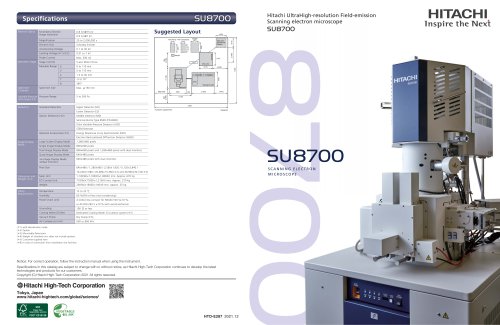
High-Resolution Field Emission SEM Life Sciences 2 Schottky Emitter Booster MD Material Contrast LD Topography 3D NAND flash memory Material contrast in the SE image An example of the high detection performance of the SU8700. This data clearly shows the structure of very thin (<10nm) nitrate, oxide and poly-Si layers in the SE image. Detection of various signals The precipitates along the grain boundaries are clearly visible when capturing SE images with the UD (upper image), while grain size and deformation are easily recognisable when capturing the BSE channeling contrast (lower image). Hi-Pixel...
Open the catalog to page 14
High-Resolution Field Emission SEM 2 SU3800 / SU3900 VP-SEM Product Family Perfect balance between imaging and analysis Schottky Emitter Booster MD Material Contrast LD Topography 150mm Prober-Shuttle Kleindiek PS8e on the pulled-out SU7000 stage 3 High-Resolution Field Emission SEM Mesoporous silica Voltage contrast on a chip Product Features Optional Accessories Large analytical sample chamber with many access ports for accessories, and a eucentric sample stage for samples up to 80mm height and 200mm diameter Extensive range of detectors Analytical EDX working distance of 6mm enables simultaneous...
Open the catalog to page 15All Hitachi High-Tech Europe GmbH catalogs and technical brochures
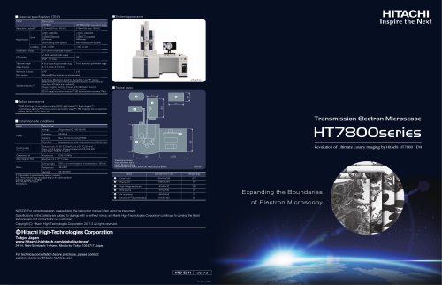 HT7800 Series | TEM
2 Pages

- HITACHI laboratory microscope
- Desktop microscope
- Sample preparation system
- Automatic sample processor
- Laboratory sample preparation system
- Benchtop sample preparation system
- Biology microscope
- HITACHI research microscope
- HITACHI high-resolution microscope
- Medical microscope
- Compact microscope
- Dark field microscope
- Inspection microscope
- 3D microscope
- Multi-function microscope
- Cooling sample preparation system
- HITACHI floor-standing microscope
- SEM microscope
- Materials research microscope