


- Company
- Products
- Catalogs
- News & Trends
- Exhibitions
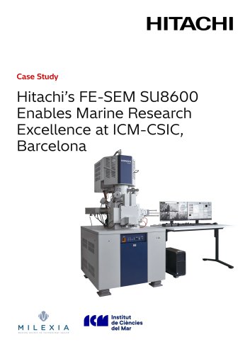
SU8600
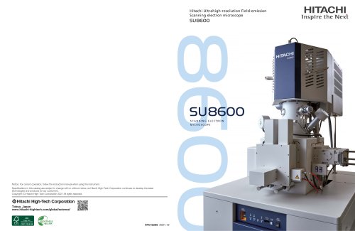
SU8600
The Hitachi SU8600 is an ultrahigh-resolution cold-field emission scanning electron microscope (CFE-SEM) designed to enhance imaging capabilities with advanced automation and user-friendly interfaces. It offers multifaceted imaging, increased system stability, and efficient workflows suitable for users of all experience levels.
The SU8600 features automated alignments and data acquisition recipes that improve efficiency, precision, and repeatability. A high-precision piezo stage enhances navigational accuracy for targeted regions of interest.
Equipped with a high-brightness cold field emission source, the SU8600 provides ultrahigh-resolution images even at low acceleration voltages. The smart detection system with ExB allows comprehensive imaging and analysis. Various detectors and options are available to meet diverse user needs.
The dual monitor configuration supports a flexible workspace, allowing simultaneous display and saving of up to six signals. High-resolution information can be acquired up to 40,960 x 30,720 pixels.
The SU8600 utilizes advanced cold field emission technology for high-resolution electron imaging. The ExB field technology enables efficient detection of secondary electrons, providing excellent signal-to-noise ratio and contrast.
The EM Flow Creator allows users to configure repeatable SEM operation sequences, enhancing data collection accuracy and repeatability. Automated optics alignment optimizes parameters for changing conditions and specimens.
The SU8600 is applicable in semiconductor, material science, and life science fields. It provides detailed imaging for semiconductor devices, material structures, and biological specimens, demonstrating its versatility and high-resolution capabilities.
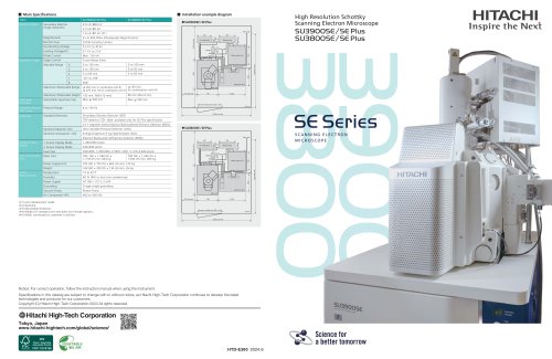
The SU8600 features a cold cathode field emission gun, a 5-axis motor drive specimen stage, and a specimen chamber accommodating up to 150mm diameter specimens. It supports various detectors and offers flexible image display modes.
The system requires specific temperature, humidity, power, grounding, cooling water, and vacuum pump conditions for optimal operation.
Catalog excerpts
Hitachi Ultrahigh-resolution Field-emission Scanning electron microscope HITACHIInspire the IMext SU8600 SCANNING ELECTRON MICROSCOPE Notice: For correct operation, follow the instruction manual when using the instrument. Specifications in this catalog are subject to change with or without notice, as Hitachi High-Tech Corporation continues to develop the latest technologies and products for our customers. Copyright (C) Hitachi High-Tech Corporation 2021 All rights reserved. ^Hitachi High-Tech CorporationTokyo, Japanwww.hitachi-hightech.com/global/science/ vO' Paper from responsible sources
Open the catalog to page 1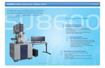
Modern Solutions for a Modern World The SU8600 brings in a new era of Ultrahigh-resolution cold-field emission scanning electron microscopes to the long-standing Hitachi EM line-up. This revolutionary CFE-SEM platform incorporates multifaceted imaging, automation, increased system stability, efficient workflows for users of all experience levels, and more. Enhanced User-Experience with Advanced Automation . Automated alignments increase efficiency and throughput. . Automated data acquisition recipes allow for greater precision as well as repeatability. . High-precision piezo stage* improves navigational...
Open the catalog to page 2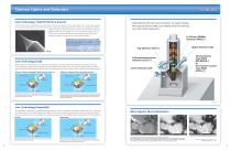
Electron Optics and Detectors Core Technology(Cold FE Electron Source) From the time that the cold field emission (CFE) electron source was realized in 1972, Hitachi High Tech has constantly improved this outstanding technology for high-resolution electron imaging. The latest developments in electron gun designs yield higher irradiation stability of the electron beam within the high-brightness region. The SU8600 enables high S/N imaging even at low accelerating voltages, and can also be used in long-term measurements and analyses under large current irradiation conditions rivaling other gun technologies...
Open the catalog to page 3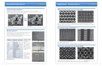
Automated Workflows Application - Semiconductor - Voltage Contrast Images of 5 nm process SRAM Automated Optics Alignment SEM operation requires optimization of various parameters when conditions, specimen, or analyses change. The SU8600 features an automated alignment function to assist in this procedure. From beam alignment to stigmator alignment, each alignment optimization can be done automatically. Above Left: W contact Layer, acquired at 0.5 kV (UD), Above Right: Co-W contact layer, acquired at 0.3 kV (TD) with deceleration condition. Various conditions such as landing energy, detector...
Open the catalog to page 4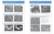
Application - Material Science - Fine Surface Structure of RHO-type Zeolite Left: RHO-type Zeolite particle at low-kV. In order to reveal fine steps structure on surface, the image was acquired at 0.8 kV of landing voltage. This allows the very fine structure of surface steps to be clearly visible (image on right). Specimen courtesy of Dr. Yoshihiro Kamimura, National Institute of Advanced Industrial Science and Technology (AIST), Japan Application - Life Science - Backscattered electron images above from ultrathin section of Arabidopsis thaliana. Images were acquired at 2 kV of acceleration...
Open the catalog to page 5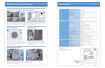
Flexible Interface and Chamber Dual monitors with 6-signal simultaneous display Electron Optics 1, 2, 4 or 6 signals, including the chamber scope(*) or SEM MAP, can be displayed simultaneously on a single monitor. By adding a second screen, the dual-monitor configuration supports enhanced productivity plus expanded workspace and allows the operation panel to be customized with submenus positioned anywhere on either screen. Camera Navigation* Detectors The built-in optical camera captures the specimen holder overview which is automatically transferred to the SEM MAP screen for a graphical navigation...
Open the catalog to page 6All Hitachi High-Tech Europe GmbH catalogs and technical brochures
 ZoneSEM II & ZoneTEM II
3 Pages
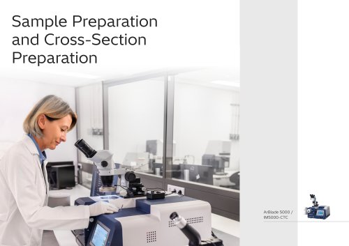 IM5000
4 Pages
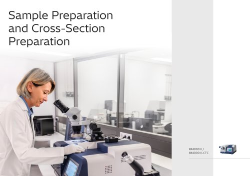 IM4000II
4 Pages
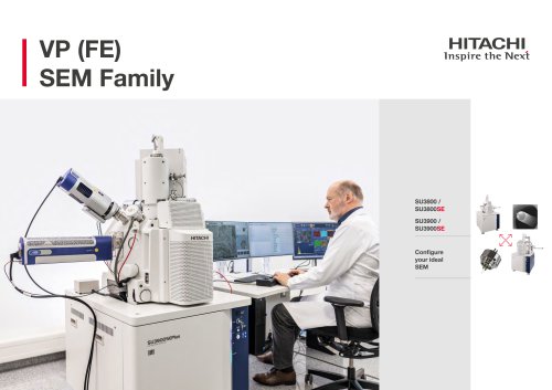 SU3800/SU3900 Family
4 Pages
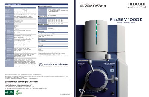 FlexSEM II
10 Pages
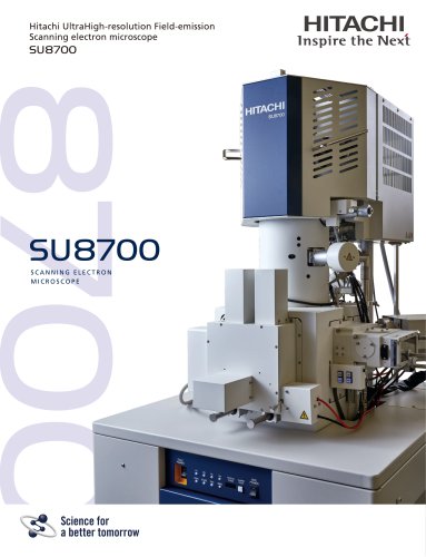 SU8700
12 Pages
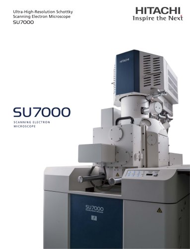 SU7000
8 Pages
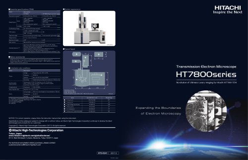 HT7800 Series | TEM
2 Pages


Archived catalogs
- Analysis software
- HITACHI laboratory microscope
- Desktop microscope
- Sample preparation system
- Automatic sample processor
- Control software
- Laboratory software
- Laboratory sample preparation system
- Benchtop sample preparation system
- Acquisition software
- Biology microscope
- Spectrophotometer
- HITACHI research microscope
- Image analysis software
- Research software
- HITACHI high-resolution microscope
- Medical microscope
- Compact microscope
- Inspection microscope