
- Catalogs
- HORIBA Scientific
- Tm PlstForm


Tm PlstForm
Tm PlstForm
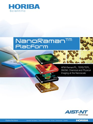
The document introduces the NanoRamanTM platform, which integrates advanced techniques like AFM-Raman/PL, TERS/TEPL, and SNOM for nanoscale chemical and physical imaging. It discusses the evolution of Scanning Probe Microscopy (SPM) since the 1980s and its enhancement through Raman spectroscopy.
- Multi-Sample Analysis Platform: Capable of macro, micro, and nanoscale measurements.
- Ease of Use: Fully automated with quick setup.
- True Confocality: High spatial resolution with automated mapping stages.
- High Collection Efficiency: Multiple detection configurations for optimal resolution.
- High Spectral and Spatial Resolution: Nanoscale spectroscopic resolution via TERS and TEPL.
- Multi-Technique/Environment Compatibility: Supports various SPM modes and environments.
- Robustness/Stability: High resonance frequency AFM scanners ensure performance without active vibration isolation.
The platform supports simultaneous SPM and spectroscopic measurements, high numerical aperture objectives, and a broad range of detection wavelengths. It includes an IR laser diode for AFM feedback and features easy tip replacement and alignment.
Examples include co-localized AFM-Raman imaging, TERS imaging, and analyses of lipid crystals, graphene structures, and silicon chips. TERS is highlighted for enhanced Raman signal detection.
Researchers emphasize the platform's versatility, ease of use, and capability for advanced nanoscale research, with applications in electrochemistry and nanomaterial characterization.
The NanoRamanTM platform is a powerful tool for nanoscale imaging and analysis, offering comprehensive material characterization through multiple techniques.
- Spec-TopTM Mode: Patented TERS imaging mode for direct surface contact measurements.
- Dual-Spec Mode: Allows subtraction of far-field from near-field maps for pure TERS images.
- Multi-Area Analysis: Selects trapezoidal areas for efficient Raman mapping.
- Curves Map: Facilitates spectroscopic and force curves for local stiffness or adhesion distribution characterization.
The platform is used for research on carbon-based nanomaterials, particularly graphene oxide for energy applications. It is user-friendly, stable, versatile, and fully automated.
Prof. Masamichi Yoshimura from Toyota Technological Institute praises the system's stability, versatility, and technical support.
HORIBA Scientific, part of Jobin Yvon established in 1819, is a leading manufacturer of analytical and spectroscopic systems, offering worldwide training and technical support.
Contact details for global offices are provided, with more information available at www.horiba.com/scientific or [email protected].
Catalog excerpts
Explore the future Automotive Test Systems I Process & Environmental I M dical I Semiconductor I Scientific
Open the catalog to page 1
Nano TM Raman Key Features ULTI-SAMPLE ANALYSIS PLATFORM M Macro, micro and nano scale measurements can be performed on the same platform. ASE OF USE E Fully automated operation, start measuring within minutes, not hours! RUE CONFOCALITY T High spatial resolution, automated mapping stages, full microscope visualization options. HIGH SPATIAL RESOLUTION Nanoscale spectroscopic resolution (down to 10 nm) through Tip-Enhanced Optical Spectroscopies (TERS: Tip-Enhanced Raman Spectroscopy and TEPL: Tip-Enhanced Photoluminescence). XploRA Nano: OmegaScope AFM combined with XploRA Raman microscope Powerful...
Open the catalog to page 2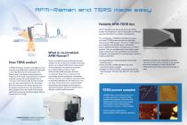
AFM-Raman and TERS made easy Reliable AFM-TERS tips Reflection Configuration OmniTM Tip-Enhanced Raman Spectroscopy TERS probes* are designed to acquire topography and Raman spectral information of a sample simultaneously. Raman scattering Field Enhancement Raman scattering Transmission Configuration How TERS works? In TERS, the Raman excitation laser is focused at the tip of an SPM probe coated with either gold or silver . Matching the wavelength of the Raman laser to the natural surface plasmonic frequency of the noble metal generates an intense localized evanescent electromagnetic fied or...
Open the catalog to page 3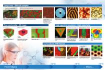
Large area - difficult samples Forsterite 1 Forsterite 2 Enstatite Whitlockite Anorthite Rhodonite Silicon Carbide Raman image - Mineral - Macro map across a sectioned meteorite Raman image - Sectioned pharmaceutical tablet Automatic panoramic AFM (contact mode) – 120 scans – CoCr features on Si surface Sample courtesy of Dr A.N. Shokin, NIIFP; Image courtesy of Dr A. Temiryazev, IRE RAS. True confocality - 3D maps Bead Raman image - XYZ volume map of expanded polymer bead in matrix AFM (topography) – 3D Top Mode imaging - Optical Fiber 6 µm AFM (topography) - MFM – Ferrite garnet film AFM (topography)...
Open the catalog to page 4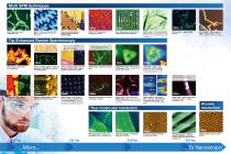
9 µm AFM – Bacillus Cereus vegetative cells MFM - Yttrium Iron Garnet (YIG) film Sample courtesy of Dr A.V. Maryakhin 2 µm Lateral Force Modulation – Polymer-fullerene blend (P3HT:PCBM) KPFM – DTP (pentacene derivative) on gold 1 µm Nano Lithography – Vector force scratching on polycarbonate AFM in liquid – Virus like particles (VLP) Sample courtesy of Prof. O. V. Karpova (Lomonosov Moscow State University) AFM in liquid – plasmid DNA on mica AFM (height) – DNA origami on mica –Sample courtesy of Prof. Michael Norton, Marshall University Tip-Enhanced Raman Spectroscopy CH stretching (Polymer)...
Open the catalog to page 5
Integrated Software NanoRaman data acquisition with ONE software Key Features NE SOFTWARE for the acquistion of AFM, O Raman and Photoluminescence signals in TERS/TEPL and AFM-Raman/PL co-localized measurements. LabSpec 6 SPECTROSCOPY SUITE for Integrated Multivariate and high level analysis at a touch of a button. PCA, MCR, HCA, DCA. NIQUE IMAGING MODES and U processing, including: Spec-TopTM mode Patented TERS imaging mode: TERS measurement is performed when the tip is in direct contact with the surface, transition between the pixels of the map is performed in semicontact mode, which preserves...
Open the catalog to page 6
Find out more at www.horiba.com/nanoraman Worldwide Training and Technical Support Jobin Yvon, established in 1819, and now part of the HORIBA Scientific is one of the world's largest manufacturers of analytical and spectroscopic systems and components. The HORIBA Scientific teams are committed to serving our customers with high performance products and superior technical support. Our staff of experienced application and service engineers, located around the world, provides full support for your instrument and its future upgrades. Well equipped application laboratories allow for sample analysis...
Open the catalog to page 7All HORIBA Scientific catalogs and technical brochures
 Ultima Expert LT
3 Pages

Archived catalogs
 LSH
LSH2 Pages
 iHR
iHR6 Pages
 LabRAM Odyssey
2 Pages
 Aqualog®
2 Pages
 MicOS
MicOS2 Pages
 BRO ICP NEO
3 Pages
 FluoroMax Plus
20 Pages
 QuantaMaster
28 Pages
 SA-9600_Series_Brochure
2 Pages
 Ultima Expert LT
3 Pages
 Ultima Expert
5 Pages
 XploRA Series
8 Pages
 LabRAM HR Evolution
5 Pages
 MacroRAM™
2 Pages
 Modular Raman Spectrometers
5 Pages
 NanoRaman brochure
7 Pages
 Tunable PowerArc
2 Pages
 Tunable KiloArc
2 Pages
 PowerArc™
2 Pages
 KiloArc
2 Pages
 EasyLife L
2 Pages
 EasyLife X
2 Pages
 MicroHead 3000
4 Pages
 MINI-CCT+
2 Pages
 THz-Raman®
4 Pages
 UVISEL Plus In-Situ
4 Pages
 Duetta™
8 Pages
 OpenPlex
2 Pages
 SZ-100
8 Pages
 LA-960V2
8 Pages
 EMGA-920
4 Pages
 LAQUAtwin
12 Pages
 LA-350
4 Pages
 LAQUAact-DO110 LAQUAact-DO120
87 Pages


- Compound microscope
- HORIBA laboratory microscope
- HORIBA benchtop microscope
- Laboratory testing system
- HORIBA spectrometer
- LED light source
- Control analyser
- Temperature testing system
- HORIBA benchtop spectrometer
- Research microscope
- Compact light source
- Fluorescence microscope
- Digital microscope
- High-resolution microscope
- Pressure testing system
- Achromatic microscope
- Microscope light source
- Compact spectrometer
- Inverted microscope