- Catalogs
- Intan Technologies
- RHS2000 USB/FPGA Interface: RhythmStim

RHS2000 USB/FPGA Interface: RhythmStim
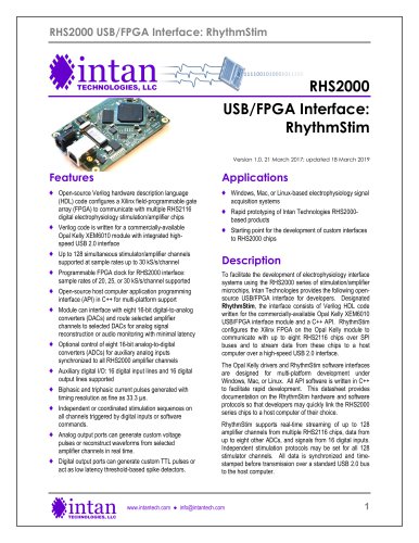
RHS2000 USB/FPGA Interface: RhythmStim
- Supports up to 128 stimulator/amplifier channels at sample rates up to 30 kS/s/channel.
- Programmable FPGA clock for sample rates of 20, 25, or 30 kS/s/channel.
- Open-source API in C++ for multi-platform support (Windows, Mac, Linux).
- Interfaces with eight 16-bit DACs and ADCs for analog signal reconstruction and auxiliary inputs.
- Generates biphasic and triphasic current pulses with a timing resolution of 33.3 µs.
- Supports independent or coordinated stimulation sequences triggered by digital inputs or software commands.
- createCommandListSingleRegisterConfig: Generates a list of 128 commands to update a single RAM register.
- createCommandListSetStimMagnitudes: Creates a list of 128 commands to set stimulation magnitudes and trim parameters for a channel.
- createCommandConfigChargeRecovery: Generates a list of 128 commands to set charge recovery current limit and target voltage.
- Constructor: Allocates memory for data blocks supporting specified data streams.
- getSamplesPerDataBlock: Returns the constant SAMPLES_PER_DATA_BLOCK, set to 128.
- calculateDataBlockSizeInWords: Computes the size of a USB data block in 16-bit words for enabled data streams.
- fillFromUsbBuffer: Fills data block with raw data from a USB input buffer.
- print: Outputs contents of RHS2116 registers from a selected USB data stream to the console.
- write: Writes data block contents to a binary output stream in little endian format.
- checkUsbHeader: Verifies USB header against a fixed "magic number" for data synchrony.
Catalog excerpts
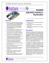
RHS2000 USB/FPGA Interface: RhythmStim RHS2000 USB/FPGA Interface: RhythmStim Version 1.0, 21 March 2017; updated 18 March 2019 ♦ Open-source Verilog hardware description language (HDL) code configures a Xilinx field-programmable gate array (FPGA) to communicate with multiple RHS2116 digital electrophysiology stimulation/amplifier chips ♦ Verilog code is written for a commercially-available Opal Kelly XEM6010 module with integrated highspeed USB 2.0 interface ♦ Up to 128 simultaneous stimulator/amplifier channels supported at sample rates up to 30 kS/s/channel ♦ Programmable FPGA clock for RHS2000 interface: sample rates of 20, 25, or 30 kS/s/channel supported ♦ Open-source host computer application programming interface (API) in C++ for multi-platform support ♦ Module can interface with eight 16-bit digital-to-analog converters (DACs) and route selected amplifier channels to selected DACs for analog signal reconstruction or audio monitoring with minimal latency ♦ Optional control of eight 16-bit analog-to-digital converters (ADCs) for auxiliary analog inputs synchronized to all RHS2000 amplifier channels ♦ Auxiliary digital I/O: 16 digital input lines and 16 digital output lines supported ♦ Biphasic and triphasic current pulses generated with timing resolution as fine as 33.3 ps. ♦ Independent or coordinated stimulation sequences on all channels triggered by digital inputs or software commands. ♦ Analog output ports can generate custom voltage pulses or reconstruct waveforms from selected amplifier channels in real time. ♦ Digital output ports can generate custom TTL pulses or act as low latency threshold-based spike detectors. ♦ Windows, Mac, or Linux-based electrophysiology signal acquisition systems ♦ Rapid prototyping of Intan Technologies RHS2000-based products ♦ Starting point for the development of custom interfaces to RHS2000 chips Description To facilitate the development of electrophysiology interface systems using the RHS2000 series of stimulation/amplifier microchips, Intan Technologies provides the following open-source USB/FPGA interface for developers. Designated RhythmStim, the interface consists of Verilog HDL code written for the commercially-available Opal Kelly XEM6010 USB/FPGA interface module and a C++ API. RhythmStim configures the Xilinx FPGA on the Opal Kelly module to communicate with up to eight RHS2116 chips over SPI buses and to stream data from these chips to a host computer over a high-speed USB 2.0 interface. The Opal Kelly drivers and RhythmStim software interfaces are designed for multi-platform development under Windows, Mac, or Linux. All API software is written in C++ to facilitate rapid development. This datasheet provides documentation on the RhythmStim hardware and software protocols so that developers may quickly link the RHS2000 series chips to a host computer of their choice. RhythmStim supports real-time streaming of up to 128 amplifier channels from multiple RHS2116 chips, data from up to eight other ADCs, and signals from 16 digital inputs. Independent stimulation protocols may be set for all 128 stimulator channels. All data is synchronized and time-stamped before transmission over a standard USB 2.0 bus to the host computer. www.intantech.com • [email protected] intan TECHNOLOGIES
Open the catalog to page 1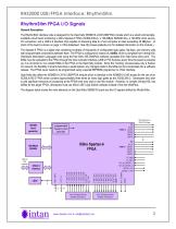
RHS2000 USB/FPGA Interface: RhythmStim RhythmStim FPGA I/O Signals General Description The RhythmStim interface code is designed for the Opal Kelly XEM6010-LX45 USB/FPGA module which is a small commerciallyavailable circuit board containing a Xilinx Spartan-6 FPGA (XC6SLX45-2), a 128-MByte SDRAM chip, a 100-MHz clock source, I/O connectors, and a USB 2.0 interface chip capable of streaming data to a host computer at rates exceeding 20 MByte/s. (A photo of the board is shown on page 1 of this datasheet. See http://www.opalkelly.com for detailed information on this module.) The Spartan-6 FPGA is...
Open the catalog to page 2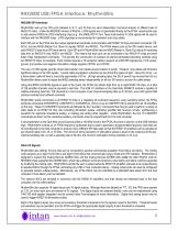
RHS2000 USB/FPGA Interface: RhythmStim RHS2000 SPI Interfaces RhythmStim sets up four SPI ports (labeled A, B, C, and D) that can send independent command streams to different sets of RHS2116 chips. Unlike the RHD2000 version of Rhythm, LVDS signals are not generated directly by the FPGA, requiring the user to add external CMOS-to-LVDS interfacing chips (e.g., the SN65LVDT41 from Texas Instruments) if LVDS signals will be used to interface with the RHS2000 chips. LVDS signaling is recommended for operation over long cables. Each SPI port on the FPGA has four output signals that coordinate communication...
Open the catalog to page 3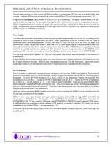
RHS2000 USB/FPGA Interface: RhythmStim The Opal Kelly board has an array of eight red LEDs (in addition to a green power LED) that may be controlled by the host computer. Additional FPGA pins are allocated for the control of eight SPI port LEDs and three general-purpose status LEDs. A digital output signal sample_clk is provided on FPGA pin L51P as a convenience. This signal is a clock running at the perchannel amplifier sampling rate. The duty cycle of the signal is 1/20. For example, if the board is configured to sample each RHS2116 amplifier channel at 20 kS/s then the period of this clock...
Open the catalog to page 4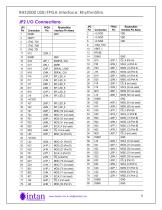
RHS2000 USB/FPGA Interface: RhythmStim www.intantech.com • [email protected]
Open the catalog to page 5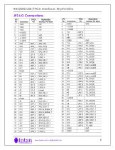
RHS2000 USB/FPGA Interface: RhythmStim www.intantech.com • [email protected]
Open the catalog to page 6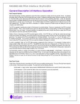
General Description of Interface Operation Host Computer Interface Most electrophysiology recording applications require that data is sampled at a steady rate for long periods of time. To interface this steady stream of data with a host computer that uses a modern, multitasking operating system requires a hardware FI FO (First In, First Out) buffer to store data during brief intervals while the computer is busy performing other tasks. Luckily, the Opal Kelly board includes a 128 MByte SDRAM chip that can be used for just such a purpose. The RhythmStim code implements an SDRAM-based FIFO as a...
Open the catalog to page 7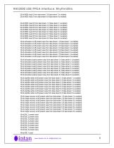
32-bit MISO result 2 from data stream 7 (if data stream 7 is enabled) 32-bit MISO result 2 from data stream 8 (if data stream 8 is enabled) 32-bit MISO result 20 from data stream 1 (if data stream 1 is enabled) 32-bit MISO result 20 from data stream 2 (if data stream 2 is enabled) 32-bit MISO result 20 from data stream 3 (if data stream 3 is enabled) 32-bit MISO result 20 from data stream 4 (if data stream 4 is enabled) 32-bit MISO result 20 from data stream 5 (if data stream 5 is enabled) 32-bit MISO result 20 from data stream 6 (if data stream 6 is enabled) 32-bit MISO result 20 from data stream...
Open the catalog to page 8