- Catalogs
- Pewatron AG
- PBM210-A11KDR_1610-21567-0025-E-0919
PBM210-A11KDR_1610-21567-0025-E-0919
1 /15Pages

PBM210-A11KDR_1610-21567-0025-E-0919
1 /15Pages
Catalog excerpts

Features □ Supply voltage: 1.7 to 5.5V(Vdd) 1.2 to 5.5V(Vddio) □ 300 to 1100 hPa pressure range □ 8cm altitude resolution (RMS) □ 2.2ms fastest conversion time □ Calibrated and temperature compensated Application Examples □ Indoor and outdoor navigation □ Weather forecast device □ Altimeter and barometer for portable device □ Bike computer Descriptions The PBM210 is a new generation of high resolution digital barometer. The PBM210 is a digital pressure sensor which consists of a MEMS piezoresistive pressure sensor and a signal conditioning ASIC. The ASIC include a 24bits sigma-delta ADC, OTP memory for calibration data, and serial interface circuits. The PBM210 could provide both I2C and SPI interface to communicate with microcontroller. Pressure calibrated and temperature compensated were key features of the PBM210. The data stored in OTP memory could be used to calibrate the PBM210. The calibration procedure should be implemented by an external microprocessor. The PBM210 is low power and supply voltage designed and suitable for portable devices or battery-supplied ones. Ordering information Competitive sensor & power supply solutions worldwide
Open the catalog to page 1
Competitive sensor & power supply solutions worldwide
Open the catalog to page 2
1 Functional Block and Pin Descriptions Competitive sensor & power supply solutions worldwide
Open the catalog to page 3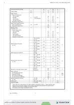
1. All the data were measured with 2.5V supply voltage at a temperature of 25±3°C, unless otherwise noted. 2. Maximum error of pressure reading over the pressure range after offset adjusted at one pressure point. 3. Maximum error of pressure reading over the pressure range. 4. According to 32 bit integer compensation formula. Competitive sensor & power supply solutions worldwide
Open the catalog to page 4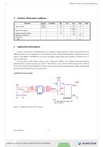
4 Application Information Owing to state of the art, the PBM210 build a new standard of digital barometer. A 24bits sigma-delta ADC and a MEMS pressure sensor are integrated in a LGA substrate. Pressure calibrated and temperature compensated were key features of the PBM210. The PBM210 is low power and supply voltage designed and suitable for portable devices or battery-supplied ones. The data stored in OTP memory could be used to calibrate the PBM210. The calibration procedure should be implemented by a external microprocessor. By I2C or SPI interface, you can get the calibration data stored...
Open the catalog to page 5
5 Control registers Table 5.1 control registers Reg 0xF6-0xF8 Data_out: 24 bits ADC output data Reg 0xF4 OSR<1:0>: 00:1024X, 01:2048X, 10:4096X, 11:8192X Measurement_control<5:0>: 101110, indicate a temperature conversion. 110100, indicate a pressure conversion. Reg 0xE0 Softreset : Write only register. If set to 0xB6, will perform a power on reset sequence. Auto returned to 0 after the soft reset completed. Reg {0xF1, 0xD0, 0xBB:0xAA} Calibration Registers : Total 20bytes calibration registers used for sensor calibration. Rev. 2.2 2019/9/4 6 Competitive sensor & power supply solutions worldwide...
Open the catalog to page 6
Reg 0x6B PartID: 8 bits Part ID, the default value is 0x42. Reg 0x00 SDO_active: 1: 4-wire SPI, 0: 3-wire SPI LSB_first: 1: LSB first for SPI interface, 0: MSB first for SPI interface Table 5.2 Summary of instructions Competitive sensor & power supply solutions worldwide
Open the catalog to page 7
Figure 6.1 SPI timing diagram The falling edge of CSB, in conjunction with the rising edge of SCLK, determines the start of framing. Once the beginning of the frame has been determined, timing is straightforward. The first phase of the transfer is the instruction phase, which consists of 16 bits followed by data that can be of variable lengths in multiples of 8 bits. If the device is configured with CSB tied low, framing begins with the first rising edge of SCLK. The instruction phase is the first 16 bits transmitted. As shown in Figure 6.2, the instruction phase is divided into a number of bit...
Open the catalog to page 8
This can be one or more bytes of data. All data is composed of 8-bit words. Data can be sent in either MSB-first mode or LSB-first mode (by setting ‘LSB_first’ bit). On power up, MSB-first mode is the default. This can be changed by programming the configuration register. In MSB-first mode, the serial exchange starts with the highest-order bit and ends with the LSB. In LSB-first mode, the order is reversed. (Figure 6.3) CSB \I scl n a a a a a a a a a a a a a a a a a a a a a a a a a a a a a a a SDIO DON'T CARE \ R/W W1 | W0 | A12 | A11 | A10 | A9 | A8 | A7 | A6 | A5 | A4 | A3 | A2 | A1 | A0 |...
Open the catalog to page 9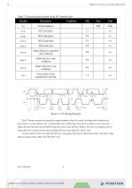
Table 7.2 Electrical specification of the I2C interface pins The I2C interface protocol has special bus signal conditions. Start (S), stop (P) and binary data conditions are shown below. At start condition, SCL is high and SDA has a falling edge. Then the slave address is sent. After the 7 address bits, the direction control bit R/W selects the read or write operation. When a slave device recognizes that it is being addressed, it should acknowledge by pulling SDA low in the ninth SCL (ACK) cycle. At stop condition, SCL is also high, but SDA has a rising edge. Data must be held stable at SDA when...
Open the catalog to page 10
START ADDRESS RAN ACK condition 8 Package Information 8.1 Outline dimensions All dimensions are in mm. Competitive sensor & power supply solutions worldwide
Open the catalog to page 11
8.3.2 Sensor orientation relative to the tape 9 Document history and modification Rev. Competitive sensor & power supply solutions worldwide
Open the catalog to page 12
Schematic figure of pin definitions, page 3 Relative pressure accuracy, page 4 Absolute pressure accuracy, page 4 Application circuit, page 5 8.1 Outline dimension, page 11 8.2 Recommended footprint, page 11_ Modified: SPI waveform, Fig. 6.1, Fig. 6.2, Fig. 6.3, Fig. 6.4 Register table, description related to 0xF4, page 6 I2C address “1101111”^”1101101”, page 9_ Modified: Figure. 4.1 Application circuit for I2C interface, page 5 8.3.2 Sensor orientation relative to the tape, page 12_ Modified: Product photo, page 1_ Added: 8ms pressure conversion time, page 1 Modified: Function block diagram:...
Open the catalog to page 13
Competitive sensor & power supply solutions worldwide
Open the catalog to page 14All Pewatron AG catalogs and technical brochures
 PEI-S103-1- 0.6 Inclinometer
2 Pages
 IPPS-015_1610-21499-0001-D-0714
13 Pages
 SLP35_1610-21567-0004-E-1017
16 Pages

