
- Catalogs
- TE Connectivity
- MS5525DSO

- Products
- Catalogs
- News & Trends
- Exhibitions
MS5525DSO
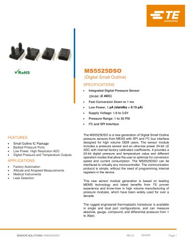
MS5525DSO
Catalog excerpts
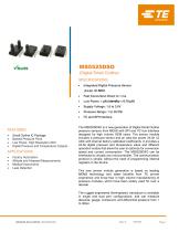
• Small Outline IC Package • Barbed Pressure Ports • Low Power, High Resolution ADC • Digital Pressure and Temperature Outputs • Factory Automation • Altitude and Airspeed Measurements • Medical Instruments • Leak Detection MS5525DSO(Digital Small Outline)SPECIFICATIONS • Integrated Digital Pressure Sensor (24-bit AI ADC) • Fast Conversion Down to 1 ms • Low Power, 1 pA (standby < 0.15 pA) • I2C and SPI Interface The MS5525DSO is a new generation of Digital Small Outline pressure sensors from MEAS with SPI and I2C bus interface designed for high volume OEM users. The sensor module includes a pressure sensor and an ultra-low power 24-bit AI ADC with internal factory calibrated coefficients. It provides a 24-bit digital pressure and temperature value and different operation modes that allow the user to optimize for conversion speed and current consumption. The MS5525DSO can be interfaced to virtually any microcontroller. The communication protocol is simple, without the need of programming internal registers in the device. This new sensor module generation is based on leading MEMS technology and latest benefits from TE proven experience and know-how in high volume manufacturing of pressure modules, which have been widely used for over a decade. The rugged engineered thermoplastic transducer is available in single and dual port configurations, and can measure absolute, gauge, compound, and differential pressure from 1 to 30psi. SENSOR SOLUTIONS ///MS5525DSO REV E 09/2024 Page
Open the catalog to page 1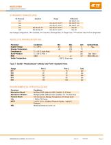
(Digital Small Outline) FS Pressure Absolute Gauge Differential See Package Configurations: DB= Dual Barb, DH= Dual Hole, SB=Single Barb, ST=Single Tube, FT=Front Side Tube, FB=Front Single Barb Solder Temperature 250°C, 5 sec max.Table 1- BURST PRESSURE BY RANGE AND PORT DESIGNATION. Range ENVIRONMENTAL SPECIFICATIONSParameter Conditions Mechanical Shock Mil Spec 202F, Method 213B, Condition C, 3 Drops Mechanical Vibration Mil Spec 202F, Method 214A, Condition 1E, 1 Hr Each Axis Thermal Shock 100 Cycles over Storage Temperature, 30 minute dwell Life 1 Million FS Cycles MTTF >10Yrs, 70 °C, 10...
Open the catalog to page 2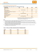
MS5525DSO (Digital Small Outline) Unless otherwise specified: Supply Voltage1 3.0 VDC, Reference Temperature: 25°CPARAMETERS MIN TYP MAX UNITS Operating Voltage 1.8 3.6 Pressure Accuracy Total Error Band (TEB) Temperature Accuracy (Reference Temperature) Temperature Accuracy Supply Current Compensated Temperature Operating Temperature Conversion Time Non-Corrosive Dry Gases Compatible with Silicon, Glass, LCP, RTV, Gold, Thermo-Epoxy, Silicone Gel, Aluminum and Epoxy. See “Wetted Material by Port Designation” chart. Notes 1. Proper operation requires an external capacitor placed as shown in Application...
Open the catalog to page 3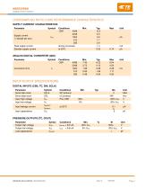
MS5525DSO (Digital Small Outline) Parameter Symbol Conditions Min. Typ. Peak supply current during conversion 1.4 Standby supply current at 25°C 0.02 Supply current ANALOG DIGITAL CONVERTER (ADC) Parameter Symbol Conditions Min. PRESSURE OUTPUTS (I2C, DOUT) Parameter Symbo Conditions Min. Ty M Unit Output high voltage Voh Isource = 0.6 mA 80% Vdd 100% V Output low voltage Vol Isink = 0.6 mA 0% Vdd 20% Vdd V Load capacitance Cload 1 pF
Open the catalog to page 4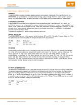
(Digital Small Outline) The MS5525DSO consists of a piezo-resistive sensor and a sensor interface IC. The main function of the MS5525DSO is to convert the uncompensated analog output voltage from the piezo-resistive pressure sensor to a 24-bit digital value, as well as providing a 24-bit digital value for the temperature of the sensor. FACTORY CALIBRATION Every module is individually factory calibrated at two temperatures and three pressures. As a result, six coefficients necessary to compensate for process variations and temperature variations are calculated and stored in the 128-bit PROM of...
Open the catalog to page 5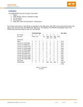
(Digital Small Outline) The MS5525DSO has only five basic commands: 2. Read PROM (128 bit of calibration words) 5. Read ADC result (24 bit pressure / temperature) Size of each command is 1 byte (8 bits) as described in the table below. After ADC read commands the device will return 24 bit result and after the PROM read 16bit result. The address of the PROM is embedded inside of the PROM read command using the Ad2, Ad1 and Ad0 bits. Figure 1: Command structure
Open the catalog to page 6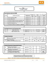
(Digital Small Outline) Read Calibration Data from PROM Variable C1 C2 Coefficient Description Pressure Sensitivity | SENST1 Pressure Offset | OFFT1 Recommended Variable Type Example/ Typical Temperature Coefficient of Pressure Sensitivity | TCS Temperature Coefficient of Pressure Offset | TCO Reference Temperature | TREF Temperature Coefficient of Temperature | TEMPSENS Read Digital Pressure and Temperature Data D1 Digital Pressure Value Digital Temperature Value Difference between actual and reference temperature dT = D2 - TRE F = D2 - C5 * 2Q5 Calculate Temperature Compensated Pressure OFF...
Open the catalog to page 7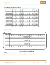
(Digital Small Outline) Qx Coefficients Matrix by Pressure Range TRES Part Number MEMORY MAPPING Memory Mapping Address Figure 3: Memory PROM Mapping Maximal size of intermediate result during evaluation of variable.
Open the catalog to page 8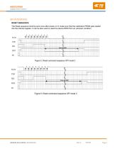
(Digital Small Outline) RESET SEQUENCE The Reset sequence shall be sent once after power-on to make sure that the calibration PROM gets loaded into the internal register. It can be also used to reset the device ROM from an unknown condition
Open the catalog to page 9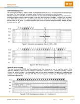
(Digital Small Outline) CONVERSION SEQUENCE The conversion command is used to initiate uncompensated pressure (D1) or uncompensated temperature (D2) conversion. The chip select can be disabled during this time to communicate with other devices. After the conversion, using ADC read command the result is clocked out with the MSB first. If the conversion is not executed before the ADC read command, or the ADC read command is repeated, it will give 0 as the output result. If the ADC read command is sent during conversion the result will be 0, the conversion will not stop and the final result will...
Open the catalog to page 10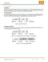
(Digital Small Outline) Each I2C communication message starts with the start condition and it is ended with the stop condition. The MS5525DSO address is 111011 Cx, where C is the complementary value of the pin CSB. Since the IC does not have a microcontroller inside, the commands for I2C and SPI are quite similar. The reset can be sent at any time. In the event that there is not a successful power on reset this may be caused by the SDA being blocked by the module in the acknowledge state. The only way to get the MS5525DSO to function is to send several SCLKs followed by a reset sequence or to...
Open the catalog to page 11All TE Connectivity catalogs and technical brochures
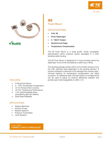 85
855 Pages
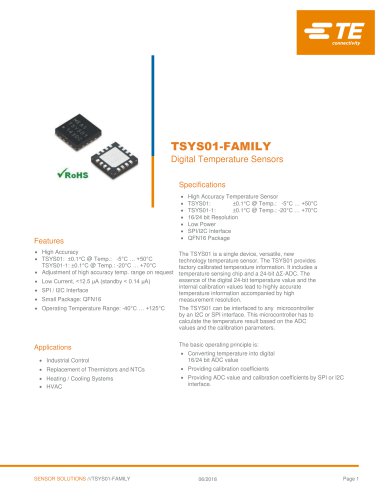 TSYS01-FAMILY
11 Pages
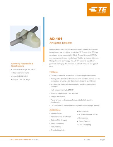 AD-101
2 Pages

Archived catalogs
 TE Sensor Solutions
4 Pages
 HTU21D
22 Pages
 CONTACT MICROPHONE CM-01B
3 Pages
 AD-101
2 Pages
 MS5525DSO
22 Pages

- Medical sensor
- SpO2 sensor
- Temperature sensor
- Monitoring sensor
- Disposable SpO2 sensor
- Latex-free SpO2 sensor
- Detector
- Process sensor
- Adhesive SpO2 sensor
- Pressure transducer
- Infant SpO2 sensor
- Disposable sensor
- Miniature sensor
- Detector for medical applications
- Compact detector
- Encoder
- Signal encoder
- Vacuum pressure transducer